.svg)


-
Technology

-
VCSEL Chips
-
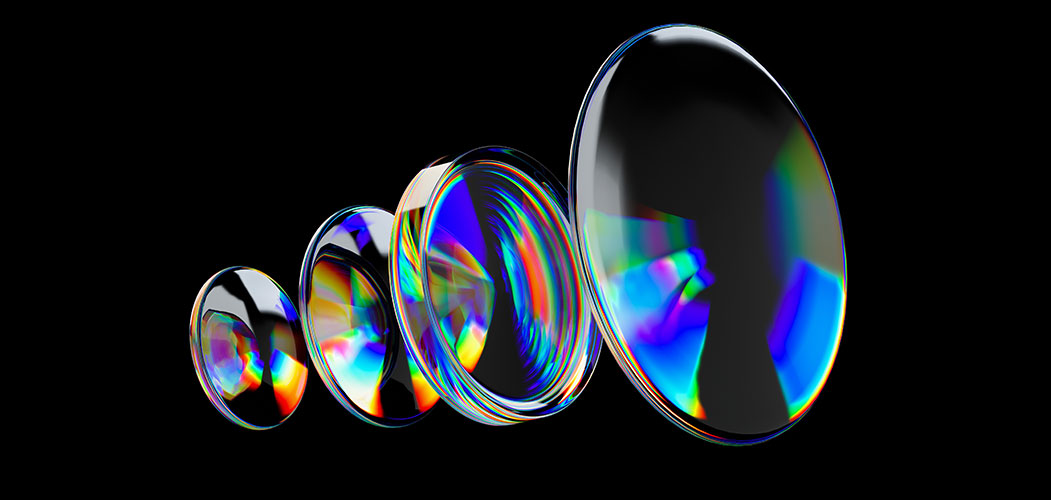
Optical Integration
-
System Integration
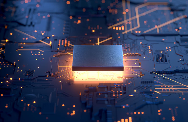
VCSEL Chips
Our in-house VCSEL epitaxial design, device design and packaging ability guarantee high performance and mass production and high reliability of our VCSEL chip products.
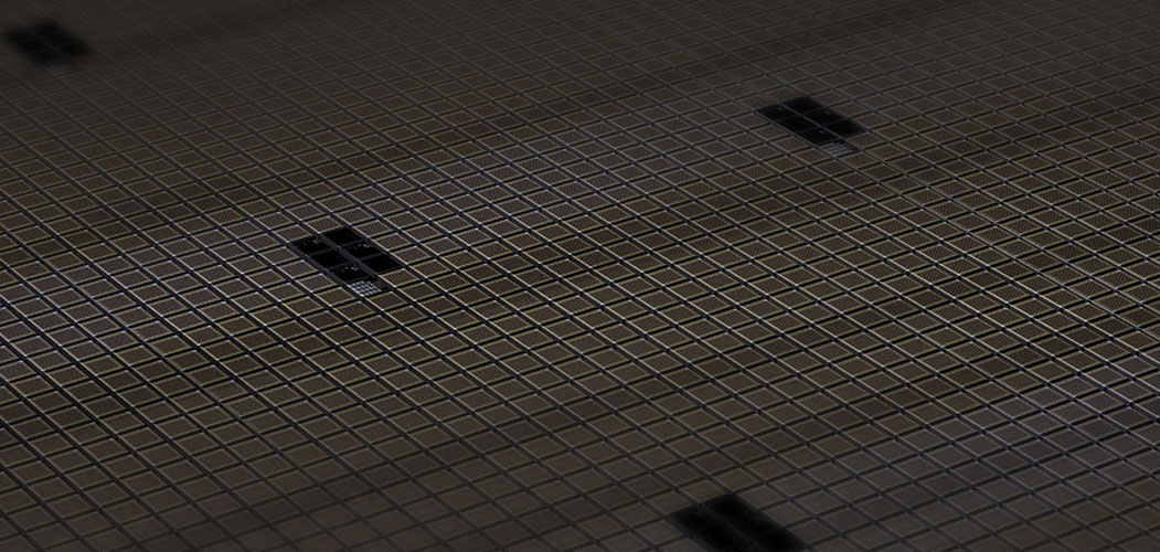

Optical Integration
First introduced in 2018, our innovative 1.5th optical integration technology combines the conventional primary optics and secondary optics into a compact package.
System Integration
To explore a wider range of applications for VCSEL depends on how to make the most use of VCSEL by integrating VCSEL with different optical components and sensors, thereby making them adapt to various optical sensing and illumination scenarios.